J-link Jlink J-tag Segger Arm 7 9 11 V9 A9a8 V9.4
em 12x
Estoque disponível
Confira a
90 dias de garantia de fábrica.


Características principais
Marca | Genérica |
|---|
Descrição
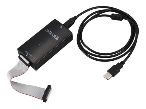
Programador Compatível com J-link Jlink J-tag Segger Arm
Baixo custo, tamanho compacto , alta performance e interface amigável
Não requer fonte de alimentação externa
J-Link V9
JTAG/SWD Emulator com Interface USB
Caracteristicas
USB 2.0 interface
Suporta CPUs: ARM7/9/11, Cortex-A5/A8/A9, Cortex-M0/M1/M3/M4, Cortex-R4
Serial Wire Debug (SWD) support
Serial Wire Viewer (SWV) support
Automatico ao reconhecer core
Velocidade JTAG até 12 MHz
Velocidade de Download até 720 Kbytes/segundo (ARM7 @ 50 MHz, velocidade 12MHz JTAG)
Integração entre IAR e Workbench IDE
Alimentado via USB
J-Link Flash Breakpoints
J-Flash
J-Link GDB Server
J-Link SDK
J-Link Flash SDK
J-Link ARM RDI
J-Link RDI/GDB-Server bundle
J-Link Pro bundle
J-Link J-Flash bundle
Flash Breakpoints no yes no
GDB Server no yes no
RDI yes yes no
J-Flash no yes yes
Especificações
Geral
Sistema operacional
Microsoft Windows 2000
Microsoft Windows XP
Microsoft Windows XP x64
Microsoft Windows 2003
Microsoft Windows 2003 x64
Microsoft Windows Vista
Microsoft Windows Vista x64
Windows 7
Windows 7 x64
Compatibilidade eletromagnética (EMC) EN 55022, EN 55024
Temperatura de operação +5°C ... +60°C
Temperatura de armazenagem -20°C ... +65 °C
Humidade Relativa (sem condensação) Max. 90% rH
Mecanico
Medidas (sem cabos) 100mm x 53mm x 27mm
Peso sem cabos 70g
Interfaces
USB interface USB 2.0, full speed
Target interface JTAG 20-pin (14-pin adapter available)
Electrico
Fonte de energia USB
Max. 50mA + Target Supply current.
Target interface voltage (VIF) 1.2V ... 5V
Target supply voltage 4.5V ... 5V (if powered with 5V on USB)
Target supply current Max. 300mA
Reset Type Open drain. Can be pulled low or
tristated.
Reset low level output voltage (VOL) VOL <= 10% of VIF
For the whole target voltage range (1.8V <= VIF <= 5V)
LOW level input voltage (VIL) VIL <= 40% of VIF
HIGH level input voltage (VIH) VIH >= 60% of VIF
For 1.8V <= VIF <= 3.6V
LOW level output voltage (VOL) with a load of 10 kOhm VOL <= 10% of VIF
HIGH level output voltage (VOH) with a load of 10 kOhm VOH >= 90% of VIF
For 3.6 <= VIF <= 5V
LOW level output voltage (VOL) with a load of 10 kOhm VOL <= 20% of VIF
HIGH level output voltage (VOH) with a load of 10 kOhm VOH >= 80% of VIF
JTAG/SWD Interface, Timing
SWO sampling frequency Max. 6MHz
Data input rise time (Trdi) Trdi <= 20ns
Data input fall time (Tfdi) Tfdi <= 20ns
Data output rise time (Trdo) Trdo <= 10ns
Data output fall time (Tfdo) Tfdo <= 10ns
Clock rise time (Trc) Trc <= 10ns
Clock fall time (Tfc) Tfc <= 10ns